Research activity
Production and characterization of nanostructured materials, including the study of diamond-like carbon films (DLC) and their alloys, graphene and other 2D materials.
Relevance / Impacts
More than fifteen doctors have been trained in the Laboratory, besides several masters and postdoc fellows trained in other institutions of Brazil, Mexico and Spain. More than 100 publications in international journals that have been cited about three thousand times have provided great national and international visibility to the laboratory, as evidenced by the various invited invitations to lectures at various national and international scientific congresses. The generation of this knowledge allowed the Laboratory to establish international collaborations with groups from the University of Verona (Italy) and Birmingham (UK), as well as research contracts with companies such as PETROBRAS and VALE. Since 2010, the Laboratory has been the headquarters of the National Institute of Science and Technology_Surface Engineering.
Brief history
The Protective Coatings and Nanostructured Materials Laboratory began its activities in 1994 focusing on the production and chemical and structural characterization of carbon-based films and other nanostructured coatings. The Laboratory has studied mechanical and tribological properties of thin films such as hardness, friction and wear seeking to establish a relationship between these properties and the chemical composition and the microstructure of the films. In the last ten years, three CVD systems have been installed in the Laboratory. Initially they were dedicated to the production of carbon nanotubes (SWNT and MWNT) and recently they were used for the production of graphene and TMDs (Transition Metals Dichalcogenides), aiming their applications in simple devices such as gas sensors. On the other hand, the production in our laboratory of graphene oxide (GO) allowed the development of anti-corrosive coatings and nanocomposite membranes.
Infrastructure
For materials synthesis:
- Plasma assisted deposition chamber: cathodic erosion (dc- and rf-magnetron sputtering) and Plasma-Assisted Chemical Deposition (PECVD);
- Thin Film Deposition Chamber by physical techniques (PVD): thermal evaporation and by electron beam;
- Three CVD systems: pyrolysis spray; LPCVD (Low-pressure CVD); APCVD (Atmospheric Pressure CVD);
- Oven up to 900 ° C for heat treatment in high vacuum or in controlled atmospheres;
- Plasma cleaner;
- Politrix for the preparation of metal surfaces;
- Ultrasound tip for solids dispersion;
- Ultra-centrifuge;
- Shimadzu precision analytical balance;
For materials characterization:
- Hysitron Nanoindentator TriboIndenter;
- CSM’s CALOWEAR micrometer rotating ball wear system;
- Goniometer for measuring contact angle of the Rame-Hart;
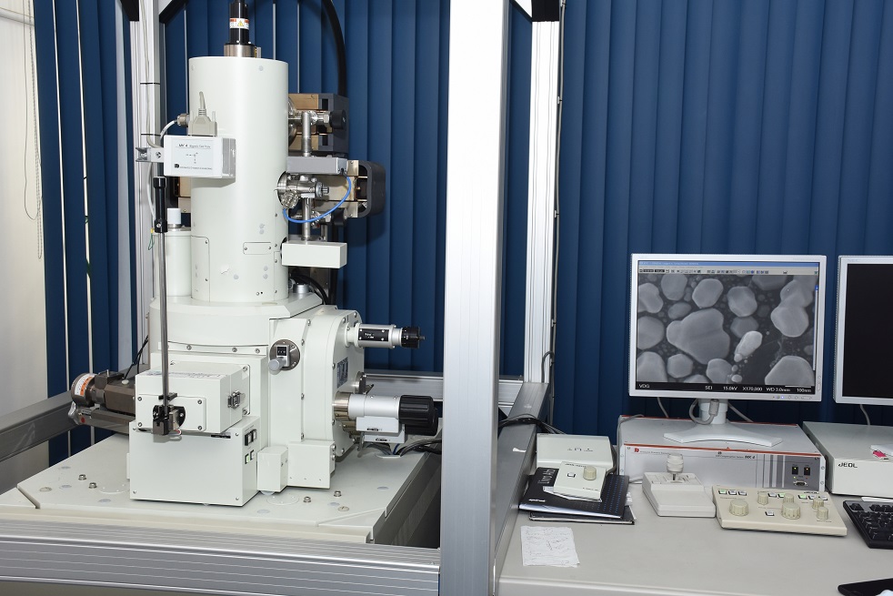
- FEG (Field emission gun) scanning electron microscope equipped with EDS and STEM JEOL model JSM-6701F;
- Optical microscopes: direct (ZEISS AXIO) and inverted (Olympus);
- Scanning Tunneling Microscope, SPM UHV, Omicron;
- Atomic Force Microscope and Coupled Raman Spectrometer – NT-MDT Spectra NTegra System;
- Infrared Spectrometer Brucker model ALPHA FTIR;
- Profilometer Brucker Dektak XT 10;
- Electrical measurements Signatone;
- Surface analysis chamber equipped with XPS technique from VG Thermo equipped with semispherical electron analyzer with 110 cm radius Alpha 110.
Contact
Fernando Lázaro Freire Jr.
Email: lazaro@vdg.fis.puc-rio.br
Tel: 21 3527-1272 ramal 219
Marcelo Eduardo Huguenin Maia da Costa
Email: maiacosta@vdg.fis.puc-rio.br
Tel: 21 3527-1272 ramal 218
Victor Carôzo Gois de Oliveira
Email: vcarozo@puc-rio.br
Tel: 21 3527-1272 ramal 215